Magnetic Levitation: A New Frontier in Microchip Fabrication
In the relentless pursuit of smaller, faster, and more efficient microchips, researchers and engineers are turning to some truly innovative technologies. One of the most intriguing developments in recent years is the use of magnetic levitation (maglev) in microchip fabrication. Yes, the same principle that powers futuristic high-speed trains is now being miniaturized and repurposed to shape the future of electronics.
What is Magnetic Levitation?
At its core, magnetic levitation involves suspending an object in air using magnetic forces, counteracting gravity without any physical contact. This is typically achieved through the repulsive force between magnets or the stabilization offered by electromagnetic fields. While the concept isn’t new—maglev trains have been zipping around for decades—its application in the cleanroom environments of semiconductor fabrication is a much more recent and exciting frontier.
The Cleanroom Challenge
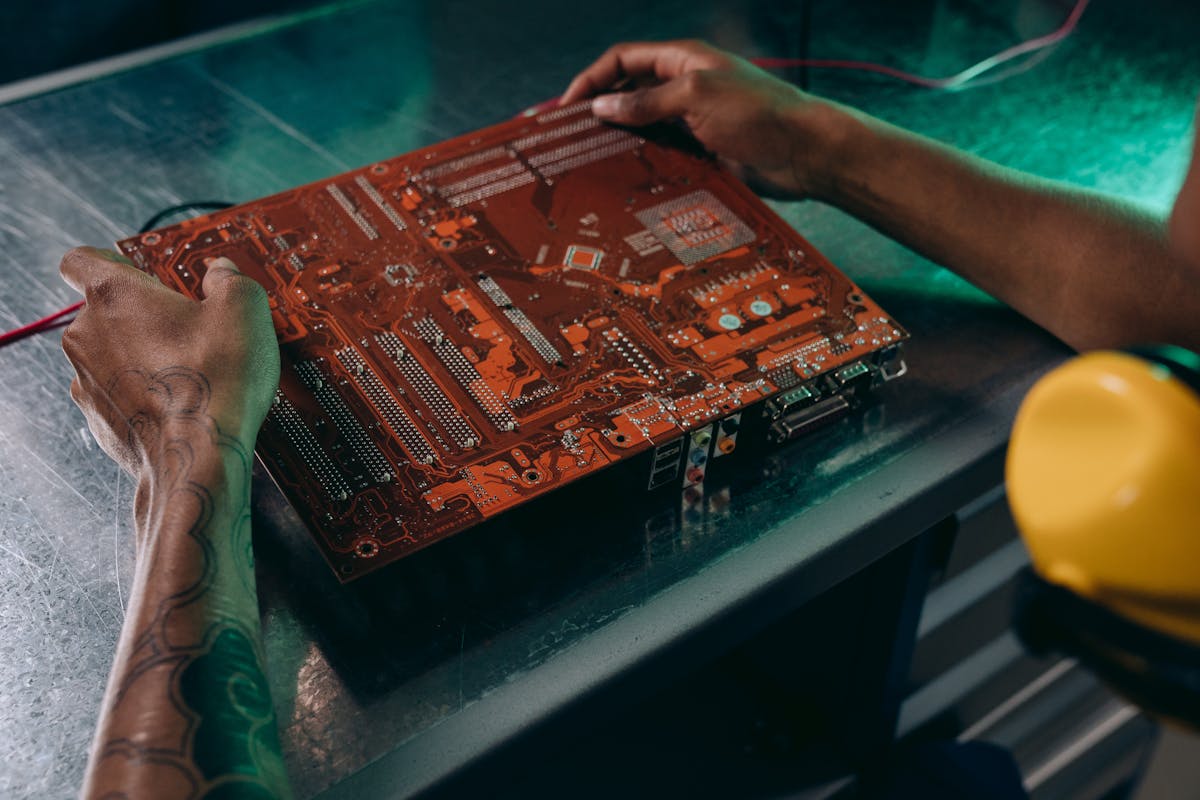
Microchip fabrication requires extremely clean and precise environments. Traditional manufacturing involves complex machinery that moves wafers (thin slices of semiconductor material) through various processing stages. These machines often rely on physical contact—rails, gears, or conveyors—to move components. But contact introduces two big problems: contamination and vibration.
Even microscopic particles or the slightest mechanical vibrations can lead to defects in chips. As components shrink to the nanoscale, the margin for error becomes virtually nonexistent. This is where maglev enters the picture.
How Magnetic Levitation Helps
Magnetic levitation offers a contactless method of handling wafers and other delicate components. Here’s how that changes the game:
- Zero Mechanical Friction: No contact means no wear and tear, reducing maintenance and extending equipment life.
- Ultra-Clean Operation: Less contact means fewer particles are generated, which keeps the environment purer and safer for sensitive chips.
- Precision Movement: Maglev systems can offer smoother and more controlled motion than mechanical systems, improving the alignment and accuracy of chip patterning and etching.
- Reduced Vibration: Levitated platforms isolate wafers from external vibrations, which is crucial during processes like photolithography where nanometer-scale precision is required.
Real-World Applications
One practical example of maglev in microchip fabrication is in wafer transport systems. Companies have begun developing maglev-based wafer handling platforms that float wafers through cleanrooms without any physical guides. This helps maintain a sterile environment while reducing the risk of breakage or contamination.
Maglev is also being explored in lithography stages, where levitated platforms can move wafers more precisely under extreme ultraviolet (EUV) light sources. The result? Finer patterns, tighter tolerances, and more powerful chips.

Challenges Ahead
Of course, integrating magnetic levitation into semiconductor fabs isn’t without challenges. It requires advanced control systems, specialized materials, and can be expensive to implement. However, as demand for high-performance chips continues to rise—with AI, 5G, and quantum computing on the horizon—the industry is more motivated than ever to invest in such futuristic solutions.
The Future is Floating
Magnetic levitation is more than a technological curiosity—it’s a practical tool that could redefine the future of chip manufacturing. By reducing contamination, improving precision, and enabling new levels of cleanliness, maglev systems could help usher in the next wave of ultra-advanced semiconductors.
As with many breakthroughs, what once seemed like science fiction is quickly becoming science fact. In the silent, dust-free chambers where tomorrow’s chips are born, the future may just be floating on magnetic fields.


